Multiparametric Electrochemical Characterisation of Te-Cu-Pb Atomic Three-Layer Structure Deposition on Polycrystalline Gold
Alexander S. Bondarenko, Genady A. Ragoisha, Nikolai P. Osipovich, Eugene A. Streltsov
Electrochem. Commun. 8 (2006) 921-926.
Physico-Chemical Research Institute, Belarusian State University, 220050 Minsk, Belarus
DOI:10.1016/j.elecom.2006.03.033.
Abstract


Successive underpotential deposition of Tead, Cuad and Pbad adlayers in the potentiodynamic mode was used for Tead/Cuad/Pbad atomic three-layer structure assembling on polycrystalline Au support. Layer-by-layer deposition was characterised in each of the stages with potentiodynamic electrochemical impedance spectroscopy (PDEIS) by variations, with the electrode potential E, of double layer pseudocapacitance Qdl, charge transfer resistance Rct and Warburg coefficient Aw of diffusion impedance. Qdl(E) has shown a strong decrease in the cathodic scan during Te atomic layer deposition on Au, a sharp peak in the subsequent Cuad deposition on Au/Tead and an increase in Pbad deposition on Au/Tead/Cuad. The inverses of charge transfer resistance and Warburg coefficient have shown characteristic maxima in Rct-1(E) and Aw-1(E) dependencies in all the three stages of Tead/Cuad/Pbad three-layer assembling. The characteristic features in the dependences on the potential of the ac response parameters compensated for insufficient self-descriptiveness of the dc part of the nonstationary interface response in the layer-by-layer deposition. High information density of PDEIS spectra provides better control of electrochemical processes on nonstationary interfaces and this new opportunity can enable wider use of electrochemical approaches for thin-layer structures preparation.
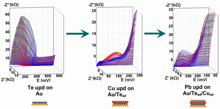
Potentiodynamic impedance spectra: red - cathodic scans (in the cathodic scans the atomic layers were formed by surface limited electrochemical deposition), blue - anodic scans (in the anodic scans the atomic layers were anodically oxidised for the investigation of irreversibility effects of the cathodic deposition). Different red and blue lines in the PDEIS spectra correspond to different ac probing frequencies.
Keywords: atomic layer, adlayer, bilayer, multilayer, tellurium, copper, lead, underpotential deposition, upd, electrodeposition, potentiodynamic electrochemical impedance spectroscopy, PDEIS, EIS, double layer capacitance, pseudocapacitance, Faradaic impedance, constant phase element, charge transfer resistance, impedance of diffusion, Warburg coefficient, impedance of adsorption, potential scan, frequency response, ac response, alternating current, 3D impedance spectrum, equivalent circuit, cyclic voltammetry, nanostructure, electrochemical nanotechnology, nanoelectrochemistry, electrochemical atomic layer epitaxy, ECALE, layer-by-layer deposition
See also full-text articles about characterisation of nonstationary electrochemical interfaces by PDEIS:
Pb upd on Au, Se upd on Au and Pb-Se bilayer electrodeposition
Variable Mott-Schottky plots acquisition by PDEIS
Articles about PDEIS